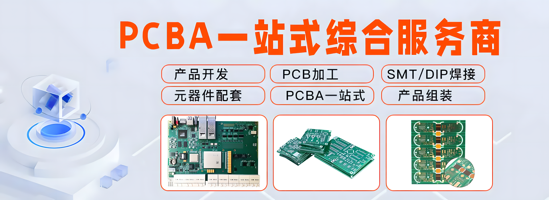
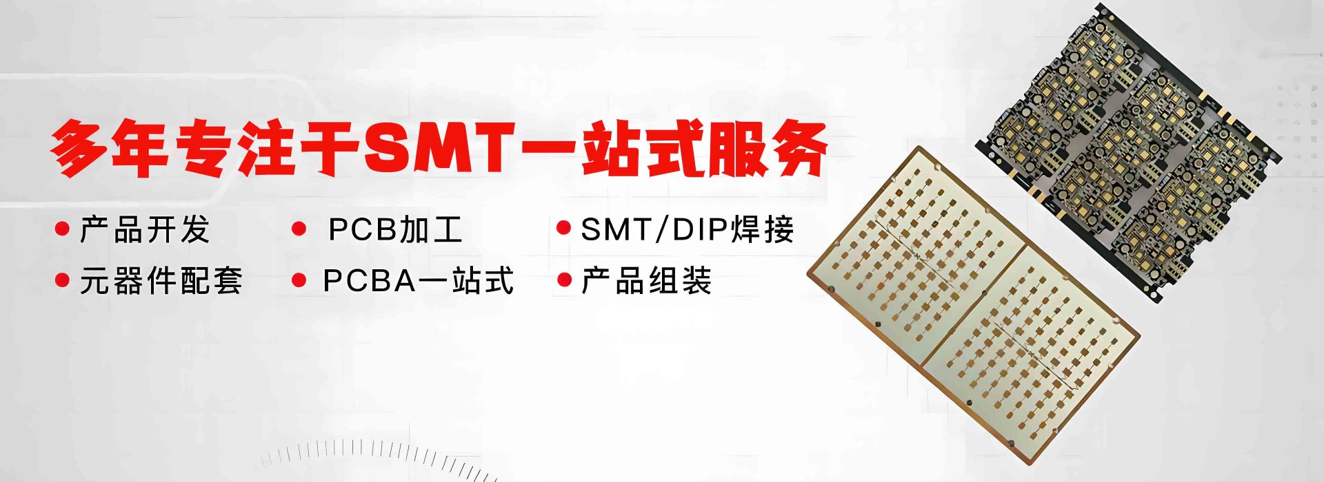

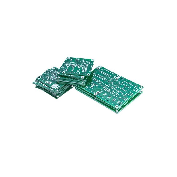

PCB (Printed Circuit Board), or printed board, is a crucial component in the electronics industry. Virtually every electronic device, from small items like wristwatches and calculators to larger ones like computers, communication equipment, and weapon systems, requires a PCB if it contains integrated circuits or other electronic components. These boards are used to facilitate electrical interconnections between various components. Composed of an insulating base, connecting conductors, and pads for mounting and soldering electronic components, PCBs serve both as conductive pathways and insulating substrates. They can replace complex wiring, enabling electrical connections between components within a circuit, thereby simplifying assembly and soldering processes, reducing the amount of wiring work, and significantly easing the physical strain on workers. Additionally, they help to shrink the overall size of the product, lower costs, and enhance the quality and reliability of electronic devices. PCBs offer excellent product consistency, allowing for standardized design and facilitating mechanization and automation during production. Moreover, a fully assembled and debugged PCB can serve as a standalone spare part, making it easier to exchange and repair whole products. Today, PCBs are widely used in the production of electronic products.
Printed circuit boards were initially based on paper with copper foil. Since the emergence of semiconductor transistors in the 1950s, the demand for PCBs skyrocketed. The rapid development and widespread application of integrated circuits have led to smaller electronic devices, increasing circuit routing density and complexity, necessitating constant PCB advancements. Currently, PCB varieties have evolved from single-sided to double-sided, multilayer, and flexible boards; structures and quality have reached ultra-high density, miniaturization, and high reliability levels; and new design methods, materials, and manufacturing processes are continually emerging. In recent years, various computer-aided design (CAD) PCB application software have become widespread and promoted in the industry, with mechanical and automated production completely replacing manual operations in specialized PCB manufacturers.
Processing Capacity:
zui
| Sample | Bulk | |
Number of Layers | 2-44L | 2-58L |
Board thickness | 0.5-17.5mm | 0.6-10mm |
Minimum mechanical aperture | 0.1mm | 02mm |
3mil | 4mil | |
HDI Type | l+n+l、 2+n+2、3+n+3 | 1+n+l、 2+n+2 |
zuiFine line width & spacing | 3/3mil | 4/4mil |
Impedance Control | +/-5% | +/-10% |
zuiLarge copper thick | 12oz | 6oz |
zuiLarge plate thick hole diameter ratio | 18:1 | 16:1 |
zuiLarge plank size | 650mm X 1130mm | 610mm X 1100mm |
Lumber | FR4/Hi-Tg/Rogers/Halogen-Free/Rcc/PTFE/Nelco/Mixed Pressing Material | |
Surface Treatment | HASL HASL PB FREE | |
| Special Processing | B埋 blind holes, step grooves, metal substrates, embedded resistors, embedded capacitors, mixed pressure, soft-hard combined, back drilling, etc. | |