
 Quartz Crystal Microbalance (QCM) - Microbial Identification and Subtyping (MIPS)
 Aluminum Ion Detector MIPS
 Fluoride Ion Detector MIPS
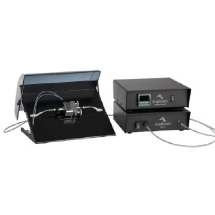 Nanoplasma Sensor Analyzer XNano
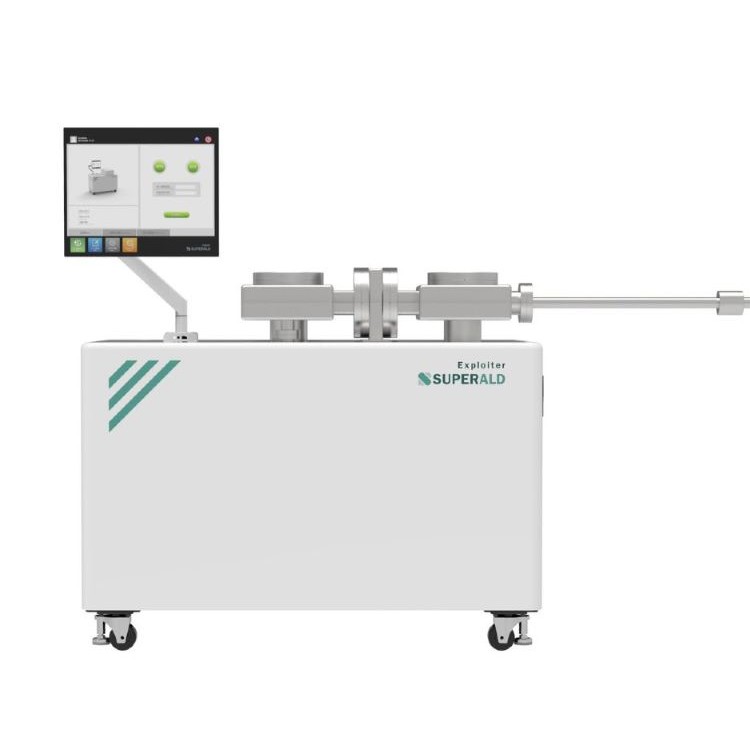 High-Vacuum Atomic Layer Deposition System UHV
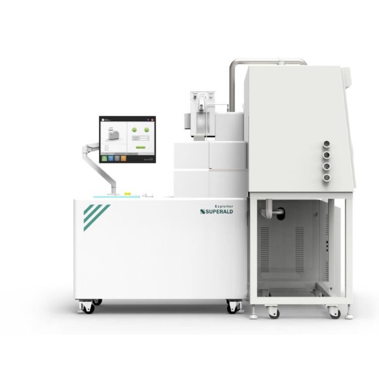 Gloved Box Integrated Atomic Layer Deposition System
 Plasma-Enhanced Atomic Layer Deposition System PEALD E200SP
Product Details

Atomic Layer Deposition Systems, Nanomechanical Testing Equipment, Molecular ...



产品Price Negotiable
最小起订Quantity:1 Tai 供货总Quantity: 100 Tai


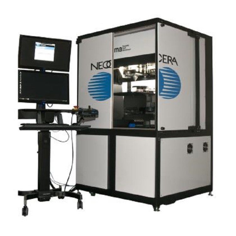
Product Information Magma Magnetic Field GeneratorThe Magma System (abbr. Magma) is a novel semiconductor failure analysis tool developed by Neocera Magma Company. It features a unique set of sensors and technology, capable of detecting and locating all static defects. Magma boasts high reliability and is suitable for detecting open circuits, short circuits, leakage, and high-resistance open circuits. Additionally, magnetic field imaging can be used to generate depth information for 3D fault analysis, and even for multi-layer devices. In the semiconductor failure analysis field, Magma can locate all static defects in microelectronic systems (shorts, leaks, and open circuits). It accommodates 300mm wafers with Die-level interconnects, packaged PC boards, and all types of packaged devices, including various multi-chip module devices with heterogeneous integration, stacked devices, 3DICs, and SiPs. The design of the new platform utilizes input from end-users to provide user-friendly settings and operations, along with higher productivity and lower operational costs. Basic Configuration: Equipped with high-sensitivity SQUID sensors for low-current, non-destructive detection of short circuits, leakage, and high-resistance open circuits. Enables low-cost localization for detecting short circuits and leaks in packaged devices and PC boards. EFI Tool: Capable of detecting open circuit faults with a high degree of precision. HiRes Tool: Combines two sensors into one tool. During proximity current scanning, the SQUID sensor is used to detect the smallest possible current, while the magneto-resistive sensor is used to achieve spatial resolution. This results in two-fold advantages: spatial localization and sensitivity. Application Fields 1. This instrument is a dual-magnetic sensor system that extends the performance of SSM tools to molds (which can be full wafer or complex 3D TSV or wire bonding equipment). The instrument creates the current image of the device at the mold, packaging, and PCB levels using non-destructive technology. Then, the current image can be combined with optical benchmarks and design data to locate three-dimensional static defects. 2. This instrument combines a high-resolution magnetoresistive sensor with the superconducting quantum interference device (SQUID). Using a two-step method, the SQUID can rapidly map the magnetic field generated by internal currents within the device, followed by a high-precision and resolution mapping with the high-resolution sensor. As most materials used in typical devices are permeable to magnetic fields, fault location can begin without any reverse processing of the device. 3. Additionally, both sensors require only a minimal current, which can protect the device under test from further damage and may be the choice when attempting to detect circuit faults with very high resistance (100k Ω). 4. The instrument can analyze typical faults such as short circuits, leaks, and open resistances. The system can be used for imaging alternating and/or direct current magnetic fields (equally, currents) depending on the equipment requirements. Technical Specifications Features Details SQUID Sensor Short-Circuit Defect Location (SCL) 3um Spatial Resolution (SQUID) 2um Total Scanning Area (SQUID) At least 100mm by 100mm
Current Sensitivity (SQUID)· 500nA @ 333um
· 1.5uA @ 1000umMagnetic Susceptibility (SQUID) 15 pT/√Hz Typical Imaging Depth (SQUID) 10mm Operating Frequency (SQUID) DC to 25kHz Opens Circuit breaker Arc Fault Location (AFL) 30um Imaging Depth (Opens) <500um Work Frequency (Opens) 20MHz to 200MHz Other Parameters Function generator ±10V @ 100mA Function generator frequency DC to 200kHz Lens Resolution 2um (in NIR or Visible)
Power Supply· 110 - 120V @ 20A
· 220 - 240V@ 10AOperating System Windows 10 64-bi 

Phone Consultation