
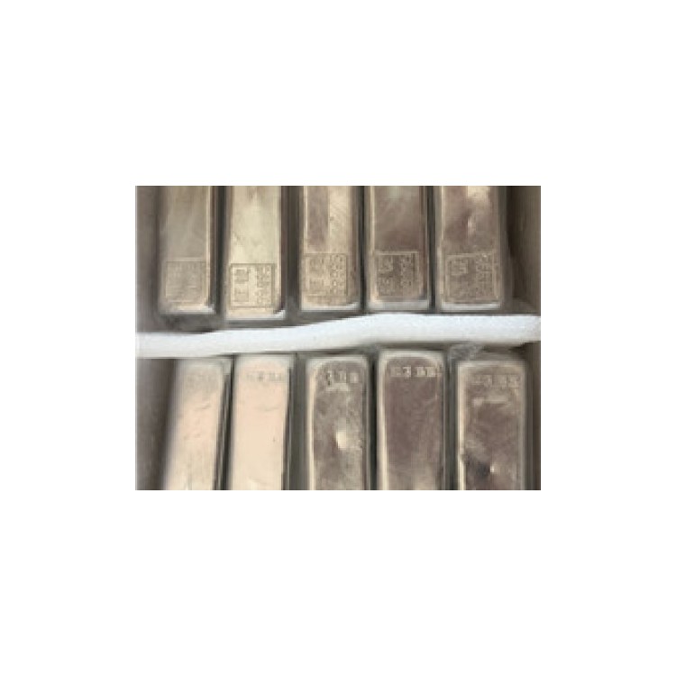






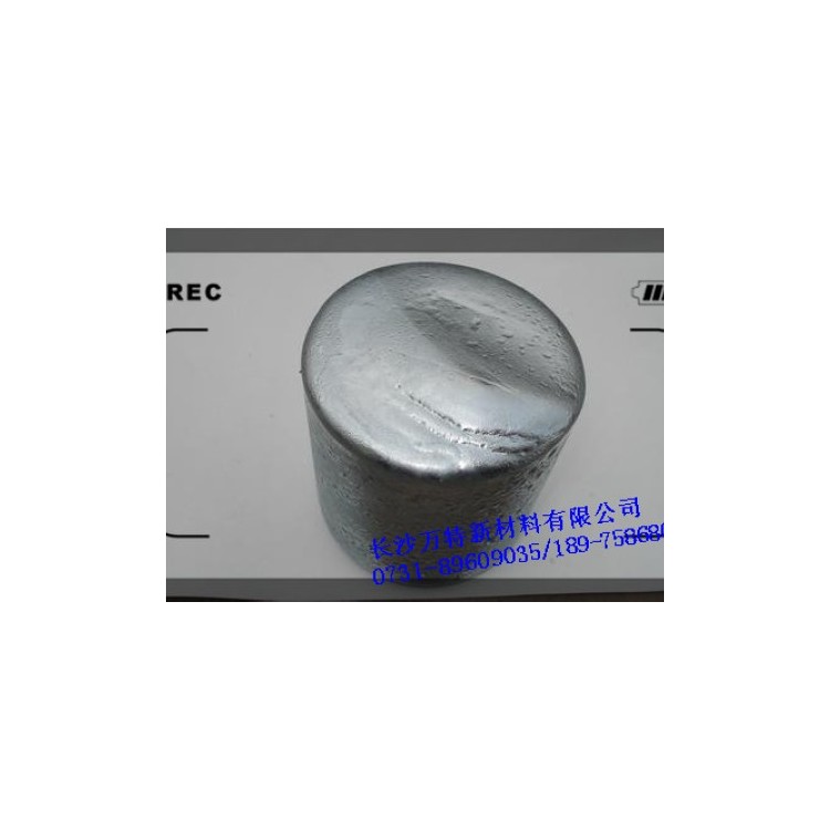
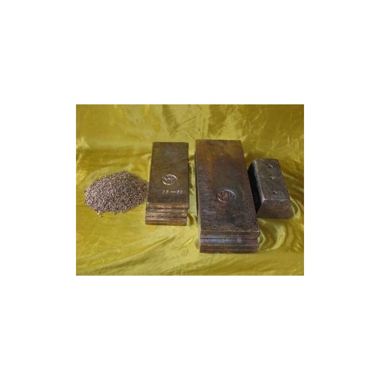
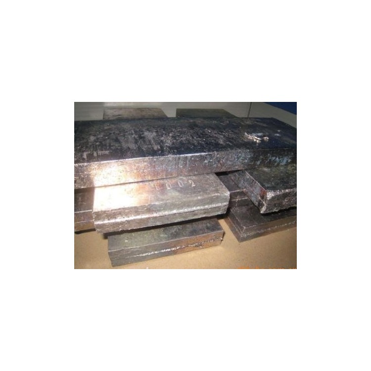
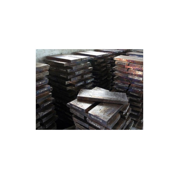
Product Name | MetalIndium ingots |
Appearance | Silver-white metal |
Specs | 500+/-50gEach ingot |
Molecular Formula | In |
Resistor | 8.37 mΩ cm |
Melting Point | 156.61℃ |
Boiling Point | 2060℃ |
Relative Density | d7.30 |
CAS No. | 7440-74-6 |
EINECS No. | 231-180-0 |
Indium is often referred to as the "vitamin of alloys." Indium alloys can be used as soldering materials, and indium is a new and important additive for lead-free solders, with the global trend towards lead-free solders benefiting the application of indium solders. Leveraging the low melting point of indium alloys, special alloys can also be produced for circuit protection devices in fire protection systems and thermal control devices in automatic control systems; a small amount of indium added to bearing alloys can extend their service life by 4-5 times compared to general bearing alloys. Indium alloys are also used in dental, steel, and non-ferrous metal corrosion-resistant decorative parts, as well as in plastic metallization.
Due to its strong corrosion resistance and reflective properties, Indium can be used to make mirrors on warships or cruise ships. Indium is sensitive to neutron radiation and can serve as a monitoring dose material in the atomic energy industry. Currently, the amount of Indium used in the atomic energy industry is roughly comparable to its usage in the electronics industry.
Indium can act as an additive in lead-acid batteries and as an inhibitor in mercury-free alkaline batteries, making them environmentally friendly. Its use in preventing the formation of a fogging layer is increasing, and the initial application of indium coatings was in the automotive industry, which may extend to industrial and residential construction. Sony Corporation in Japan has invented a new cathode using indium instead of scandium, reducing the cost of each electron to about one-tenth of that of scandium-doped electrons. Therefore, indium's application in televisions for high-power output and long life has a promising future.
In the optoelectronics field, indium and its compound semiconductors have a wide range of applications. Among the III-V compound semiconductors based on indium, such as InSb, InP, and InAs, InSb was the earliest to be researched and applied. InP, however, is highly valued and holds promising potential, making breakthroughs in microwave to millimeter-wave communication, as a laser light source for fiber-optic communication, and as a material for heterojunction solar cells. This showcases the favorable prospects of indium applications. InSb and InAs are also crucial in infrared detection and photomagnetic devices. In solar cells, indium compound thin films are gaining traction due to their high conversion rates, low cost, and portability. Copper indium selenide (CIS) and other I-II-VI ternary compound thin film semiconductor materials, with their low cost, good performance, and simple processes, are set to become a significant direction for the development of solar cell industry. The emerging new industry centered around information technology has sparked demand for indium tin oxide (ITO), a key material in various flat panel displays. Currently, about 75% of the world's indium is consumed in this area, with great potential for future growth. Moreover, with advancements in indium extraction and processing technologies, and the reduction of production costs, the applications of indium are continuously expanding.
Indium is a silver-gray, extremely soft, fusible metal. Melting point: 156.61°C. Boiling point: 2060°C. Relative density: d7.30. Molten indium can wet glass and will adhere to surfaces it contacts, leaving black stains.
Indium has slight radioactivity, with two main isotopes: In-113, a stable nucleus, and In-115, which undergoes beta decay. Therefore, it is best to avoid direct contact during use.
Indium ingots, due to their high light transmittance and conductivity, are primarily used in the production of ITO targets (used for manufacturing LCDs and flat-panel screens). This application is the main consumption field for indium ingots, accounting for 70% of the total indium consumption.
The subsequent consumer sectors include: the electronics and semiconductor field, accounting for 12% of the consumption; the solder and alloy sector, also taking up 12%; and the research industry, which constitutes 6%. Additionally, due to its softer nature, it is also used for filling seams in industries that require filling metal, such as vacuum gap filling materials at higher temperatures.
Medically, indium colloid is used for liver, spleen, and bone marrow scans. Indium-DTPA is used for brain and kidney scans. Lung scans utilize indium-Fe(OH)3 particles. Placental scans employ indium-Fe-ascorbic acid. Liver blood pool scans are performed with indium-bound transferrin.
Gallium and Indium AlloysLiquid MetalThis forms a solid solution alloy, which can become liquid at room temperature with a surface tension of 500 millinewtons per meter. This means that, without any external force, when placed on a flat surface, the alloy maintains an almost perfect spherical shape. Upon applying a small electric current, the surface tension of the sphere decreases, and the metal stretches across the surface. If the charge reverses from negative to positive, the liquid metal will reform into a sphere. Adjusting the voltage can also modify the metal's surface tension and viscosity, allowing for different structural transformations. This research can also be applied to help repair severed human nerves, preventing long-term disability. Researchers claim that this breakthrough aids in the construction of circuits and self-healing structures.