High-performance thermoplastic material modification, standard plates/rods, continuous fiber reinforced thermoplastic prepreg, thermoplastic sizing agents
0511-80260583

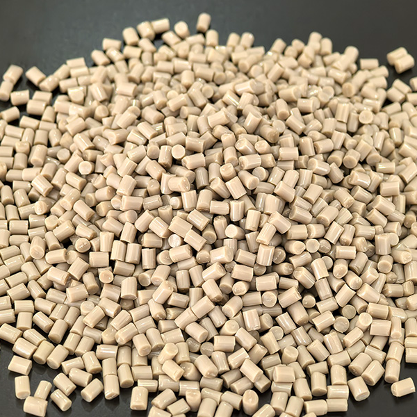
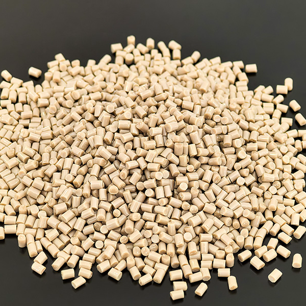
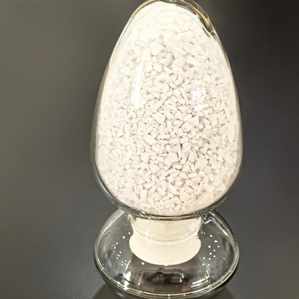
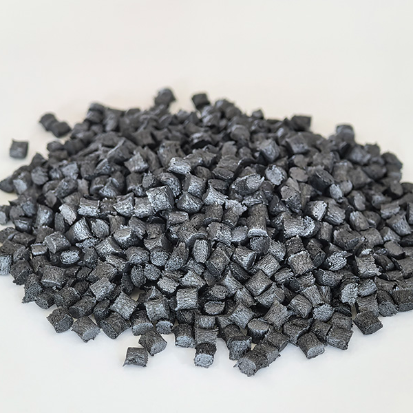
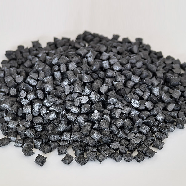
The semiconductor and electrical/electronic industries are poised to become another growth area for PEEK resin applications. In the semiconductor sector, to achieve high functionality and low cost, larger silicon wafer sizes and more advanced manufacturing technologies are required. That's where PEEK resin comes into play, with its special requirements.
Contact us

Service Hotline
17805021086
Company Telephone
0511-80260583

Address
66 Fengquan Road, Sutou Town, Danyang City, Jiangsu Province
www.114global.com © Zhongshang 114 Hebei Network Technology Co., Ltd.Address: Room 6009, Oriental New World Center, No.118 East Zhongshan Road, Qiaoxi District, Shijiazhuang City, Hebei ProvincePlatform Service Hotline: 4006299930