
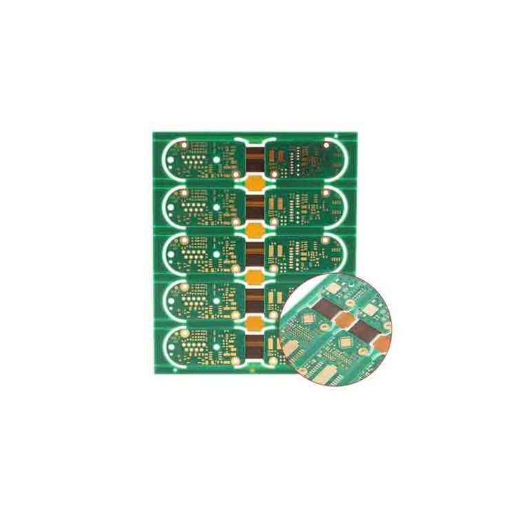


PCB (printed circuit board), or printed wiring board, is a crucial component in the electronics industry. Virtually every electronic device, from tiny electronic watches and calculators to larger computers, communication equipment, and weapon systems, requires PCBs whenever integrated circuits and other electronic components are involved. PCBs are essential for interconnecting these components electrically. They consist of an insulating substrate, connecting conductors, and pads for assembling and welding electronic components, serving both as conductive pathways and insulating bases. PCBs can replace complex wiring, facilitating electrical connections between components within circuits, simplifying assembly and soldering processes, reducing wiring work, and significantly easing labor intensity. Moreover, they help reduce the overall size of the product, lower costs, and enhance the quality and reliability of electronic devices. PCBs offer good product consistency, allowing for standardized designs that are conducive to automation and mechanization in the production process. Additionally, fully assembled and debugged PCBs can serve as independent spare parts, facilitating interchangeability and maintenance of the entire product. PCBs are now widely used in the production of electronic products.
Printed circuit boards (PCBs) were initially made using paper-based copper-clad materials. Since the emergence of semiconductor transistors in the 1950s, there has been a dramatic increase in demand for PCBs. Particularly, the rapid development and widespread use of integrated circuits have led to smaller electronic devices, with increasingly dense and complex circuit layouts. This necessitates constant updates to PCB technology. Currently, PCB varieties have evolved from single-sided to double-sided, multi-layer, and flexible boards; their structures and quality have advanced to ultra-high density, miniaturization, and high reliability levels. New design methods, materials, and manufacturing processes are continuously emerging. In recent years, computer-aided design (CAD) software for PCBs has become widespread in the industry, and in specialized PCB manufacturers, mechanized and automated production has completely replaced manual operations.
Processing Capacity:
zui
| Sample | Bulk | |
Layer | 2-44L | 2-58L |
Sheet thickness | 0.5-17.5mm | 0.6-10mm |
Minimum mechanical hole diameter | 0.1mm | 02mm |
3mil | 4mil | |
HDI Type | l+n+l、 2+n+2、3+n+3 | 1+n+l、 2+n+2 |
zuiFine Line Width & Spacing | 3/3mil | 4/4mil |
Impedance Control | +/-5% | +/-10% |
zuiLarge thick copper | 12oz | 6oz |
zuiLarge plate thick hole diameter ratio | 18:1 | 16:1 |
zuiLarge plank dimensions | 650mm X 1130mm | 610mm X 1100mm |
Lumber | FR4/Hi-Tg/Rogers/Halogen-Free/Rcc/PTFE/Nelco/Mixed Dielectric Materials | |
Surface Treatment | HASL HASL PB FREE | |
| Special Processing | Plugging blind holes, step grooves, metal substrates, embedded resistors, embedded capacitors, mixed pressure, soft-hard combination, back drilling, etc. | |